
PCB is an abbreviation for Printed Circuit Board. In some countries, PCB is called PWB (Printed Wiring Board).
A PCB includes an insulating substrate, copper foil connecting wires, and pads for electronically soldering components.
It has the dual function of wire and insulating base. It can replace complex wiring and realize the circuit connection between components in the circuit.
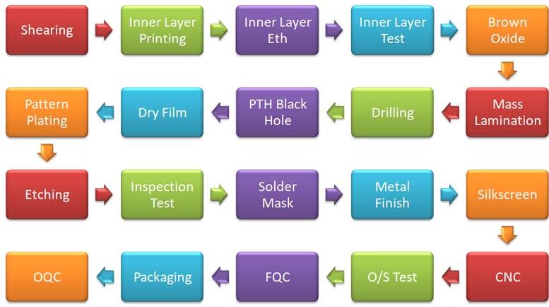
2. VIA drilling, you need to use a CNC drill to drill the VIA holes through the top and bottom layers of the PWB.
3. PCB through-hole copper plating, after drilling, the entire wall of the PCB material is free of copper, and a thin layer of copper needs to be dropped on the surface of the PCB using the copper sinking process.
4. For PWB electroplating, there is a thin layer of copper on the surface of the copper-immersed PCB, which cannot meet the requirement of 18um copper thickness at the bottom of the IPC. Therefore, it needs to be plated to improve the consistency of the drill. The factory production standard of ipcb is 20-26um.
5. PCB lamination, after lamination, press a layer of dry blue film on the printed circuit board. Dry film is a carrier that is very important in circuit technology. Therefore, the dry film process is also named after this. Compared with wet film, dry film has higher stability and better quality, and can be directly used as non-metallized via.
6. For circuit exposure, first align the circuit film with the printed circuit board, and press the dry film, then place it on the exposure machine for exposure. Under the action of the energy of the lamp tube of the exposure machine, the dry film is exposed to the place where there is no circuit film. After the PWB circuit exposure process, areas with circuits are not exposed, while areas without circuits are exposed.
7. The circuit is etched, the copper that needs the course is left, and the copper is etched away with sulfuric acid where the copper is not needed.
8. PCB solder mask by screen printing or coating with solder resist ink, and coat a layer of solder mask on the surface of the board to prevent short circuit during soldering, usually use green, blue, red, white, black solder mask.
9. PCB screen printing, print the position number of the part and the screen printing of the printed circuit board model on the printed circuit board, usually white or black screen printing.
10. PCB surface finish. Copper often exists in the form of oxides. It is prone to moisture oxidation when exposed to air for a long time. It is impossible to maintain the original copper for a long time. Therefore, surface treatment of the copper surface is required. The most basic purpose of surface preparation is to ensure good solderability or electrical performance.
11. PWB Shapping, stamping the assembled work plate PNL into SET or PCS that needs to be delivered by CNC or mold, and perform corresponding shape processing V-cutting, chamfering, step groove, tapered hole, etc.
12. PCB test, use PWB flying probe test or general test electromechanical performance to check whether there is an open circuit or short circuit NG board. Sometimes, PCB impedance test and PWB high voltage test are required.
13. FQC final inspection, check PCB appearance, size, aperture, thickness, marking, etc. to meet customer needs. Then, the qualified PWBs are shipped in vacuum packaging.